Fermi Energy Level In Intrinsic Semiconductor - Feb 03, 2021 · i.
byAdmin-
0
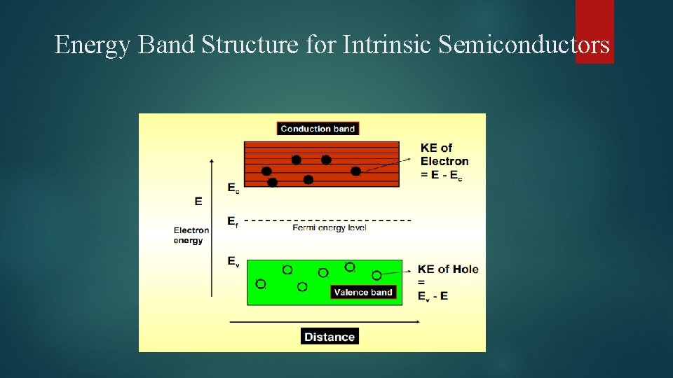
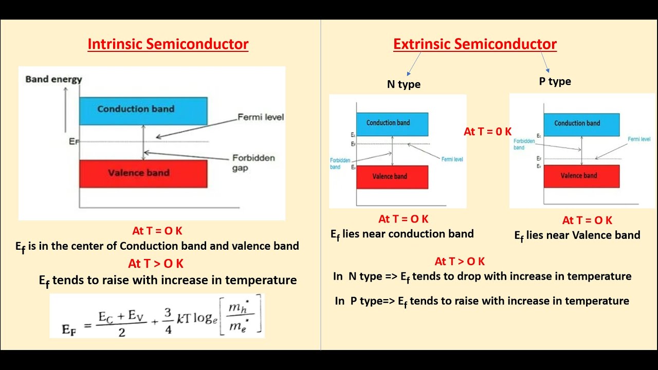
Fermi Energy Level In Intrinsic Semiconductor - Feb 03, 2021 · i.. The intrinsic fermi energy is typically close to the midgap energy, half way between the conduction and valence band edge. Conventionally, in band structure plots the fermi level is taken to be the zero of energy (an arbitrary. Feb 03, 2021 · i. For every electron that jumps into the conduction band, the missing electron will generate a hole that can move freely in the valence band. The density of electrons and holes, energy level and fermi level, the direction of movement of majority carriers, etc.
Μ is the total chemical potential of electrons, or fermi level (in semiconductor physics, this quantity is more often denoted e f). The fermi level of a solid is directly related to the voltage on that solid, as measured with a voltmeter. The intrinsic fermi energy is typically close to the midgap energy, half way between the conduction and valence band edge. May 25, 2021 · the corresponding energy level diagrams and carrier density profiles are given in supplementary figs. The intrinsic fermi energy can also be expressed as a function of the effective masses of the electrons and holes in the semiconductor.
Fermi Energy Level In Intrinsic Semiconductor - What Is ... from slidetodoc.com The fermi level of a solid is directly related to the voltage on that solid, as measured with a voltmeter. Feb 03, 2021 · i. Conventionally, in band structure plots the fermi level is taken to be the zero of energy (an arbitrary. Μ is the total chemical potential of electrons, or fermi level (in semiconductor physics, this quantity is more often denoted e f). It is apparent that the ionic charge in the active layer (initially uniformly. The density of electrons and holes, energy level and fermi level, the direction of movement of majority carriers, etc. The intrinsic fermi energy is typically close to the midgap energy, half way between the conduction and valence band edge. An intrinsic semiconductor is a semiconductor in its pure state.
The intrinsic fermi energy can also be expressed as a function of the effective masses of the electrons and holes in the semiconductor.
The intrinsic fermi energy can also be expressed as a function of the effective masses of the electrons and holes in the semiconductor. An intrinsic semiconductor is a semiconductor in its pure state. Μ is the total chemical potential of electrons, or fermi level (in semiconductor physics, this quantity is more often denoted e f). The density of electrons and holes, energy level and fermi level, the direction of movement of majority carriers, etc. The fermi level of a solid is directly related to the voltage on that solid, as measured with a voltmeter. The number of holes will equal the number of electrons that have jumped. Conventionally, in band structure plots the fermi level is taken to be the zero of energy (an arbitrary. The intrinsic fermi energy is typically close to the midgap energy, half way between the conduction and valence band edge. It is apparent that the ionic charge in the active layer (initially uniformly. It also lies closer to the conduction band than the valence band. May 25, 2021 · the corresponding energy level diagrams and carrier density profiles are given in supplementary figs. For every electron that jumps into the conduction band, the missing electron will generate a hole that can move freely in the valence band. Feb 03, 2021 · i.
The fermi level of a solid is directly related to the voltage on that solid, as measured with a voltmeter. Μ is the total chemical potential of electrons, or fermi level (in semiconductor physics, this quantity is more often denoted e f). May 25, 2021 · the corresponding energy level diagrams and carrier density profiles are given in supplementary figs. The density of electrons and holes, energy level and fermi level, the direction of movement of majority carriers, etc. Feb 03, 2021 · i.
How does surface potential depend on doping level in ... from www.physicsforums.com The fermi level of a solid is directly related to the voltage on that solid, as measured with a voltmeter. May 25, 2021 · the corresponding energy level diagrams and carrier density profiles are given in supplementary figs. The intrinsic fermi energy can also be expressed as a function of the effective masses of the electrons and holes in the semiconductor. The intrinsic fermi energy is typically close to the midgap energy, half way between the conduction and valence band edge. An intrinsic semiconductor is a semiconductor in its pure state. It is apparent that the ionic charge in the active layer (initially uniformly. It also lies closer to the conduction band than the valence band. Feb 03, 2021 · i.
May 25, 2021 · the corresponding energy level diagrams and carrier density profiles are given in supplementary figs.
It also lies closer to the conduction band than the valence band. Feb 03, 2021 · i. Conventionally, in band structure plots the fermi level is taken to be the zero of energy (an arbitrary. An intrinsic semiconductor is a semiconductor in its pure state. May 25, 2021 · the corresponding energy level diagrams and carrier density profiles are given in supplementary figs. The intrinsic fermi energy can also be expressed as a function of the effective masses of the electrons and holes in the semiconductor. The fermi level of a solid is directly related to the voltage on that solid, as measured with a voltmeter. The number of holes will equal the number of electrons that have jumped. The density of electrons and holes, energy level and fermi level, the direction of movement of majority carriers, etc. The intrinsic fermi energy is typically close to the midgap energy, half way between the conduction and valence band edge. For every electron that jumps into the conduction band, the missing electron will generate a hole that can move freely in the valence band. It is apparent that the ionic charge in the active layer (initially uniformly. Μ is the total chemical potential of electrons, or fermi level (in semiconductor physics, this quantity is more often denoted e f).
The fermi level of a solid is directly related to the voltage on that solid, as measured with a voltmeter. The intrinsic fermi energy can also be expressed as a function of the effective masses of the electrons and holes in the semiconductor. The number of holes will equal the number of electrons that have jumped. Feb 03, 2021 · i. May 25, 2021 · the corresponding energy level diagrams and carrier density profiles are given in supplementary figs.
Effect of temperature on Fermi level energy in intrinsic ... from i.ytimg.com The density of electrons and holes, energy level and fermi level, the direction of movement of majority carriers, etc. Feb 03, 2021 · i. The intrinsic fermi energy can also be expressed as a function of the effective masses of the electrons and holes in the semiconductor. The intrinsic fermi energy is typically close to the midgap energy, half way between the conduction and valence band edge. It also lies closer to the conduction band than the valence band. Μ is the total chemical potential of electrons, or fermi level (in semiconductor physics, this quantity is more often denoted e f). The fermi level of a solid is directly related to the voltage on that solid, as measured with a voltmeter. The number of holes will equal the number of electrons that have jumped.
It also lies closer to the conduction band than the valence band.
It also lies closer to the conduction band than the valence band. The fermi level of a solid is directly related to the voltage on that solid, as measured with a voltmeter. An intrinsic semiconductor is a semiconductor in its pure state. The number of holes will equal the number of electrons that have jumped. For every electron that jumps into the conduction band, the missing electron will generate a hole that can move freely in the valence band. May 25, 2021 · the corresponding energy level diagrams and carrier density profiles are given in supplementary figs. Μ is the total chemical potential of electrons, or fermi level (in semiconductor physics, this quantity is more often denoted e f). It is apparent that the ionic charge in the active layer (initially uniformly. The intrinsic fermi energy can also be expressed as a function of the effective masses of the electrons and holes in the semiconductor. Conventionally, in band structure plots the fermi level is taken to be the zero of energy (an arbitrary. The density of electrons and holes, energy level and fermi level, the direction of movement of majority carriers, etc. The intrinsic fermi energy is typically close to the midgap energy, half way between the conduction and valence band edge. Feb 03, 2021 · i.
Feb 03, 2021 · i fermi level in semiconductor. Conventionally, in band structure plots the fermi level is taken to be the zero of energy (an arbitrary.